Tuesday, May 24, 2011

SSD(Solid State Drive)

A solid state disk / drive (SSD) - is electrically, mechanically and software compatible with a conventional (magnetic) hard disk.

The difference is that the storage medium is not magnetic (like a hard disk) or optical (like a CD) but solid state semiconductor such as battery backed RAM, RRAM, PRAM or other electrically erasable RAMlike non volatile memory chip such as flash.

This provides faster access time than a hard disk, because the SSD data can be randomly accessed in the same time whatever the storage location. The SSD access time does not depend on a read/write interface head synchronising with a data sector on a rotating disk. The SSD also provides greater physical resilience to physical vibration, shock and extreme temperature fluctuations. SSDs are also imune to strong magnetic fields which could sanitize a hard drive.

The only downside to SSDs is a higher cost per megabyte of storage - although in some applications the higher reliability of SSDs makes them cheaper to own than replacing multiple failing hard disks. When the storage capacity needed by the application is small (as in some embedded systems) the SSD can actually be cheaper to buy because hard disk oems no longer make low capacity drives. Also in enterprise server acceleration applications - the benefit of the SSD is that it reduces the number of servers needed compared to using hard disk based RAID on its own.

Historically RAM based SSDs were faster than flash based products - but in recent years the performance of the fastest flash SSDs has been more than fast enough to replace RAM based systems in many server acceleration applications.

Both types of SSDs are available in a wide range of form factors and supporting traditional disk interfaces. A complete list of manufacturers with tables by form factor, technology type and interface type is updated in real-time in the Solid State Disks Buyers Guide

The reasons that users might benefit from buying SSDs are listed in the SSD Market Adoption Model

Take the case of SSD speedup in servers. One way of thinking about this concept in computer architecture is - SSD CPU Equivalency. For a wide range of applications if you take a black box approach and analyze the overall application performance of a computer system - you would not know whether that system had more CPUs with hard disks or less CPUs with more SSDs.

Implicit in all my usages of the term "flash SSD" is the assumption that the device includes some form of controller which performs wear-leveling - as opposed to less smart flash memory storage which doesn't. 

Why Use a Solid State Drive?
Solid state drives have several advantages over the magnetic hard drives. The majority of this comes from the fact that the drive does not have any moving parts. While a traditional drive has drive motors to spin up the magnetic platters and the drive heads, all the storage on a solid state drive is handled by flash memory chips. This provides three distinct advantages:
  • Less Power Usage
  • Faster Data Access
  • Higher Reliability
The power usage is a key role for the use of solid state drives in portable computers. Because there is no power draw for the motors, the drive uses far less energy than the regular hard drive. Now, the industry has taken steps to address this with drive spin downs and the development of hybrid hard drives, but both of these still use more power. The solid state drive will consistently draw less power then the traditional and hybrid hard drive.

Sunday, May 22, 2011

High End Package

QPI 1 IOH


Product Information :
Type : GA-X58A-UD3R
Price : $199.99  in Amazon
Socket : LGA1366 
SATA Feature : SATA3 
VGA SUpport : ATI CrossFireX ATX 


Product Information :
Type :  Intel Core i7 980X
Price :  $1,019.99 in Amazon
Clock Speed : 3.46GHz 
Max Turbo Frequency : 3.73 GHz
Cache :12MB 
Socket : LGA1366
Number of Simultaneous Threads : 12 (With Intel HT Technology)


Product Information : 
Type : Corsair XMS3
Price :  $68.99 in Amazon
Size : 3 x 2 GB 
PC Type : PC3-10666 
FSB :1333MHz 
Channel Support : Triple Channel Core i7 DDR3 Memory Kit 
Product Information : 
Type : GIGABYTE ATI Radeon HD5770 
2DVI/ HDMI/ DisplayPort PCI-Express Video Card, Retail GV-R577UD-1GD
Price :  $129.99 in Amazon
Size : 1 GB 
DDR Type : DDR5
VGA Support : 2DVI/ HDMI/ DisplayPort PCI-Express Video Card, Retail GV-R577UD-1GD


Confuse about Hard-Disk??
Try it!!
WD(Western Digital)

Product Information :
Type : Western Digital Caviar Black WD1001FALS
Price: $84.99 in Amazon
Capacity : 1 TB Bulk/OEM 
Size : 3.5 Inch
Speed : 7200 RPM
Cache : 32 MB 
SATA support : SATA II

 
Seagate 


Product Information :
Type :Seagate Barracuda 7200  Internal Hard Drive ST31000528AS-Bare Drive
Price: $66.99  in Amazon
Capacity : 1 TB
Speed : 7200RPM 

Cache : 32MB
Size : 3.5 Inch

Product Information : 
Type : Logitech Wireless Desktop MK320 Keyboard and Mouse
Price :  $24.99 in Amazon


Quick Path Interconnect (QPI)

The first Nehalem architecture processor release was the Core i7 for single socket desktop systems in November 2008.
The Xeon 5500 series followed in April 2009 for 2-way server systems.
Both have 4 physical cores, 3 DDR3 memory channels.
The Core i7 has a single QPI channel and the Xeon 5500 has 2 QPI.
The 2-way Xeon system can be configured with a single IOH or with two IOH as shown below.
With one IOH, both processors connected directly to the IOH.
Each IOH has two QPI channels and 36 PCI-E Gen 2 lanes plus the ESI.
With two IOH, each processor connects directly to one IOH, and the IOH also directly connected to each other.


QPI 1 IOH


QPI 2 IOH


Notice that there are 1366 pins on the Nehalem processor versus 603 or 771 for the Core 2 based Xeon
processor, and the number on pins on the IOH (now without memory channels) is reduced to a more economical 1295 pins.


The QPI has a bandwidth of 12.8GB/s in each direction simultaneously for a combined
bi-directional bandwidth of 25.6GB/s.
Each PCI-E Gen 2 lane operates at 5Gbit/sec for a net bandwidth of 500MB/s per lane, per direction.
A x4 PCI-E Gen 2 channel is rated 2GB/s per direction, and 4GB/s per direction for the x8 channel.
So while the 36 PCI-E Gen2 lanes on the 5520 IOH are nominally rated for 18GB/s per direction,
the maximum bandwidth per QPI is still 12.8GB/s per direction.
Still the dual IOH system would have a nominal IO bandwidth of 25.6GB/s per direction.
It would very interesting to see what the actual bandwidth, disk and network,
the Xeon 5500 system can sustain is.


The 4-way Nehalem architecture (which might be a Dell R910) scheduled for release in late 2009,
looks something like below.


Each processor socket
has 8 physical cores, hyper-threading (HT or 2 logical processors per core),
16M L3 cache, 4 memory channels, and 4 QPI. The architecture of the 4-way
system has each processor (socket) directly connected to all three other
processor sockets. The remaining QPI connects to an IO hub. Another difference
relative to the AMD Opteron system is that the Intel IO hub has two QPI ports,
where each connects to a processor.


Each QPI full link can be split as two half wide links.
The Nehalem EX with four full QPI can support glue-less 8-way system architecture.
Glue-less means that no other
silicon is necessary to connect the processors together.
Each processor
connects directly to all seven other processors with a half-wide QPI link, and
uses the remaining half wide QPI to connect to the IOH.
The Hyper Transport
Consortium describes this arrangement for a future Opteron system with 4 full
HT links per processor
(HT_General_Overview).
The actual 8-way system architectures described so to date do employ half-wide
links, for both current Opteron systems and forth coming Nehalem EX system.

Wednesday, May 18, 2011

Preview Intel Sandy Bridge


Sandy Bridge is the bridge to the future of processor technology. No wonder if we call it. The reason, Sandy Bridge is the biggest change since the era of Intel's Pentium 4.

In previous microarchitecture, Intel's more to optimize the performance of each component, without altering the workings of the component. If the processor is analogous as a home, Intel is just doing renovations on the house.

But in Sandy Bridge, Intel actually build a new house. All components are updated, ranging from Branch Predictor , out-of-order execution , until the working memory subsystem .

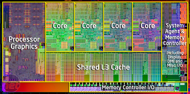
But most important is Sandy Bridge is actually a form of fusion processor , aka the processor that brings together all the components of the processor into a piece of silicon.

Actually Intel has been doing this integration policy since 2 years ago. On the generation of Bloomfield processors, they include memory controller . In Lynnfield, turn PCI-E controller the entry. The peak in the era of Clarkdale, when onboard Intel graphics chip .

There is one important note of the whole process: the whole is actually still a separate component in silicon chips are different. Well, that's what Intel Destroy in Sandy Bridge. All the components in the Sandy Bridge processor is in a piece of silicon that is made with 32nm fabrication.

The components inside the processor itself is approximately the same as Nehalem. The first course core processors. In this first generation of Sandy Bridge core number is still 2 and 4, but will be followed by the next generation who have 6 and 8 core.
Each core has L2 cache of 256KB. Work aided aided L2 cache level 3 cache (L3 cache ) an amount equal to the core with the size varied between 3-8MB, depending on the segmentation. While PCI Express, DMI, and memory controller and display interface be assembled into one component called the System Agent.

Manufacturer: Intel
UK price (as reviewed): TBC
US price (as reviewed): From $117 to $317 (ex tax)

It seems that we’ve been hearing about Intel’s next-gen CPU architecture, codenamed Sandy Bridge, for the past year, and previewing motherboards and revelling in the leaks for at least four months. In fact, it reached the point where we’d said ‘Sandy Bridge’ so often in the office that it started sounded stupid – Intel’s coming in to show us its Sandy Bridge? Wouldn’t a medical professional be more appropriate, we’d joke.

However, that all ended soon after we received our first CPU samples in November and started our own testing. Our conclusions? The Sandy Bridge CPU range is incredible, and has the potential to change the entire PC industry.

Intel Sandy Bridge Review
Intel's new CPU has the price and performance to change the PC industry

Intel hasn’t helped at all to convey the significance of its new line-up – the range is still branded Core i3, i5 and i7, making it hard to know whether it’s new at all. The Internet has also been awash with rumours that Sandy Bridge won’t overclock at all, or that it’s so easy to do so and the CPUs are so fast that Sandy Bridge will make the LGA1366 Core i7 range redundant – not bad for a mid-range, mid-priced CPU.

There’s a lot to explain when it comes to the new Sandy Bridge range, so we’ll endeavour to blow away the myths and deliver the facts as clearly and concisely as possible.

How to Spot a Sandy Bridge CPU

Intel is calling Sandy Bridge its second-generation Core architecture, which is wrong. The first Core-branded CPU was a laptop-only CPU based on the Yonah architecture of early 2006, followed by Conroe and its mobile equivalent Merom, which was sold under the Core 2 brand. Ignoring the Conroe update that was Allendale, manufacturing process shrinks of Wolfdale and Penryn, and the Core 2 Quad CPU designs, Intel should have realised that Nehalem counts as a new architecture.

We therefore reckon that Sandy Bridge is Intel’s fourth genuinely new Core architecture, not its second. It’s scandalous that Intel should throw away the excellent pedigree of the Core brand by not recognising this.

Intel Sandy Bridge Review


The lower line shows the new logo for the Sandy Bridge range – the brand is cracking apart to reveal the underlying technology, rather than peeling off as before. As Intel is erroneously calling all its Sandy Bridge CPUs its second generation of Core CPUs, every model name starts with the number ‘2’. You can also recognise a Sandy Bridge CPU by the four numerals in its model number rather than three, and any CPU with a ‘K’ at the end of its model number as a practically unlocked multiplier (it caps out at 57x, which is plenty for almost every possible use).

Standard Component

Processor


RAM


MainBoard