Sandy Bridge is the bridge to the future of processor technology. No wonder if we call it. The reason, Sandy Bridge is the biggest change since the era of Intel's Pentium 4.
In previous microarchitecture, Intel's more to optimize the performance of each component, without altering the workings of the component. If the processor is analogous as a home, Intel is just doing renovations on the house.
But in Sandy Bridge, Intel actually build a new house. All components are updated, ranging from Branch Predictor , out-of-order execution , until the working memory subsystem .
But most important is Sandy Bridge is actually a form of fusion processor , aka the processor that brings together all the components of the processor into a piece of silicon.
Actually Intel has been doing this integration policy since 2 years ago. On the generation of Bloomfield processors, they include memory controller . In Lynnfield, turn PCI-E controller the entry. The peak in the era of Clarkdale, when onboard Intel graphics chip .
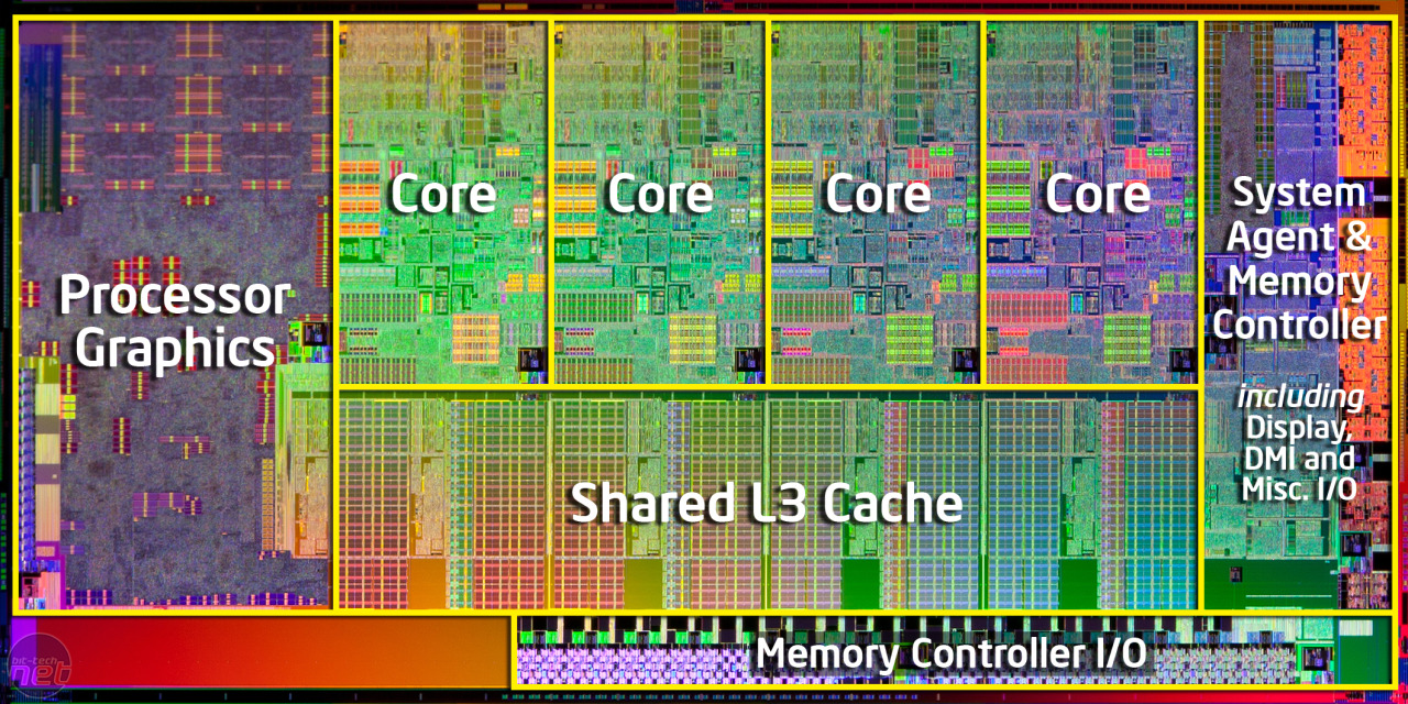
There is one important note of the whole process: the whole is actually still a separate component in silicon chips are different. Well, that's what Intel Destroy in Sandy Bridge. All the components in the Sandy Bridge processor is in a piece of silicon that is made with 32nm fabrication.
The components inside the processor itself is approximately the same as Nehalem. The first course core processors. In this first generation of Sandy Bridge core number is still 2 and 4, but will be followed by the next generation who have 6 and 8 core.
Each core has L2 cache of 256KB. Work aided aided L2 cache level 3 cache (L3 cache ) an amount equal to the core with the size varied between 3-8MB, depending on the segmentation. While PCI Express, DMI, and memory controller and display interface be assembled into one component called the System Agent.
Manufacturer: Intel
UK price (as reviewed): TBC
US price (as reviewed): From $117 to $317 (ex tax)
It seems that we’ve been hearing about Intel’s next-gen CPU architecture, codenamed
Sandy Bridge, for the past year, and previewing motherboards and revelling in the leaks for at least four months. In fact, it reached the point where we’d said ‘Sandy Bridge’ so often in the office that it started sounded stupid – Intel’s coming in to show us its Sandy Bridge? Wouldn’t a medical professional be more appropriate, we’d joke.
However, that all ended soon after we received our first CPU samples in November and started our own testing. Our conclusions? The Sandy Bridge CPU range is incredible, and has the potential to change the entire PC industry.
 Intel's new CPU has the price and performance to change the PC industry
Intel hasn’t helped at all to convey the significance of its new line-up – the range is still branded Core i3, i5 and i7, making it hard to know whether it’s new at all. The Internet has also been awash with rumours that Sandy Bridge won’t overclock at all, or that it’s so easy to do so and the CPUs are so fast that Sandy Bridge will make the LGA1366 Core i7 range redundant – not bad for a mid-range, mid-priced CPU.
There’s a lot to explain when it comes to the new Sandy Bridge range, so we’ll endeavour to blow away the myths and deliver the facts as clearly and concisely as possible.
How to Spot a Sandy Bridge CPU
Intel is calling Sandy Bridge its second-generation Core architecture, which is wrong. The first Core-branded CPU was a laptop-only CPU based on the Yonah architecture of early 2006, followed by Conroe and its mobile equivalent Merom, which was sold under the Core 2 brand. Ignoring the Conroe update that was Allendale, manufacturing process shrinks of Wolfdale and Penryn, and the Core 2 Quad CPU designs, Intel should have realised that Nehalem counts as a new architecture.
We therefore reckon that Sandy Bridge is Intel’s fourth genuinely new Core architecture, not its second. It’s scandalous that Intel should throw away the excellent pedigree of the Core brand by not recognising this.
The lower line shows the new logo for the Sandy Bridge range – the brand is cracking apart to reveal the underlying technology, rather than peeling off as before. As Intel is erroneously calling all its Sandy Bridge CPUs its second generation of Core CPUs, every model name starts with the number ‘2’. You can also recognise a Sandy Bridge CPU by the four numerals in its model number rather than three, and any CPU with a ‘K’ at the end of its model number as a practically unlocked multiplier (it caps out at 57x, which is plenty for almost every possible use).